- Phone
-
Address
No. 47 Tian'edang Road, Wuzhong District, Suzhou City, Jiangsu Province
Product Categories
Suzhou Dehui Scientific Instrument Co., Ltd

Hitachi High Tech Scanning Electron Microscope FlexSEM 1000
NegotiableUpdate on 04/18
- Model
- Nature of the Manufacturer
- Producers
- Product Category
- Place of Origin
Overview
Hitachi High Technologies Corporation released the new scanning electron microscope FlexSEM 1000 globally on April 15, 2016. This product has a compact structure and small footprint, but its resolution is not inferior to that of a large electron microscope. At the same time, it is extremely easy to operate and can be operated almost without training. Compact design with a resolution of 4 nm.
Product Details
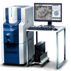
Hitachi High Technologies Corporation released a new scanning electron microscope, the FlexSEM 1000, globally on April 15, 2016. This product has a compact structure and small footprint, but its resolution is not inferior to that of a large electron microscope. At the same time, it is extremely easy to operate and can be operated almost without training. Compact design with a resolution of 4 nm.
Scanning electron microscopy can perform high magnification observation and high-precision elemental analysis on the surface of materials, and has a wide range of applications in nanotechnology, life sciences, product design and development, and failure analysis. In recent years, the demand for scanning electron microscopy to observe surface fine structures and analyze elements has been increasing, and more and more users hope to use scanning electron microscopy in limited spaces such as production lines, quality assurance inspection lines, and office areas. Therefore, scanning electron microscopes with small size, easy operation, and high resolution have attracted much attention. The FlexSEM 1000 host has a width of 450mm and a length of 640mm, reducing its volume by 52%, weight by 45%, and power consumption by 50% compared to the SU1510 model. It is also equipped with standardized power interfaces. The host and power supply unit can be separated, making installation very flexible.
The FlexSEM 1000 adopts the latest designed electronic optical system and highly reliable and sensitive detectors, with a resolution of up to 4nm. The FlexSEM 1000 has multiple automation functions and is easy to operate, allowing even first-time operators to quickly capture high-quality images. In addition, the newly developed navigation function "SEM MAP" can use various optical or electron microscope images for navigation, quickly and accurately switching to the high magnification field of interest with just one click.
characteristic:
a. By using high-sensitivity secondary electron detectors, backscatter detectors, and low vacuum detectors (UVD)*2)Realize high-quality image observation under low acceleration voltage/low vacuum conditions
b. Easy to operate, even beginners can take high-quality pictures
c. The newly developed navigation function 'SEM MAP' facilitates quick locking of the field of view
d. Large window (30mm)2)SDD energy spectrum system facilitates rapid analysis of elemental composition*2
*When set on the desktop, separate the host and power box
*2 optional options
| project | content | |
|---|---|---|
| Resolution*3 | 4.0 nm @ 20 kV (SE: High Vacuum Mode) 15.0 nm @ 1 kV (SE: High Vacuum Mode) 5.0 nm @ 20 kV (BSE: Low Vacuum Mode) |
|
| Accelerating Voltage | 0.3 kV ~ 20 kV | |
| Magnification factor | 6 ×~300000 × (film magnification) 16 ×~800000 × (display magnification) |
|
| Low vacuum mode | Vacuum range: 6-100 Pa | |
| electron gun | Centered cartridge filament | |
| sample stage | 3-axis automatic motor table X:0 ~ 40 mm, Y:0 ~ 50 mm, Z:5 ~ 15 mm R:360°, T:-15° ~ +90° |
|
| Maximum sample size | Diameter 80 mm | |
| Maximum sample height | 40 mm | |
| size | Host: 450 (W) x 640 (D) x 670 (H) mm Power supply unit: 450 (W) x 640 (D) x 450 (H) mm |
|
| Detector selection | ||
Similar Product Recommend


